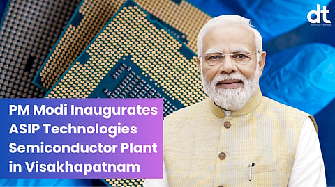

Prime Minister Narendra Modi has inaugurated ASIP Technologies’ semiconductor manufacturing facility at Tarluvada in Visakhapatnam, marking a significant milestone in India’s semiconductor manufacturing journey. The facility is the first semiconductor manufacturing unit in Andhra Pradesh and South India approved under the India Semiconductor Mission (ISM 1.0).
The semiconductor facility, developed with a total investment of ₹2,500 crore, is an Outsourced Semiconductor Assembly and Test (OSAT) unit aimed at strengthening India’s semiconductor supply chain and building domestic capabilities in advanced chip packaging technologies.
The inauguration ceremony was attended by Andhra Pradesh Chief Minister N. Chandrababu Naidu, senior government officials, industry leaders, and global technology partners. Key attendees included India Semiconductor Mission CEO Amitesh Kumar Sinha, Andhra Pradesh IT, Electronics and Communications Secretary Bhaskar Katamneni, and Special Secretary Mallavarapu Surya Teja.
Facility to Produce 96 Million Semiconductor Chips Annually
The ASIP Technologies semiconductor facility is being developed on a 30-acre site and has an initial investment of more than ₹460 crore. The project is being established in collaboration with South Korea-based APACT Co., which will serve as the technology partner for the facility.
Once operational, the plant is expected to achieve an annual production capacity of 96 million semiconductor chips. The facility will focus on semiconductor packaging solutions for emerging technology sectors, including artificial intelligence (AI), high-performance computing (HPC), data centres, and high-speed communication systems.
The project represents a major step towards expanding India’s semiconductor manufacturing ecosystem by enabling local capabilities in assembly, testing, and packaging of chips used across critical technology applications.
Advanced Packaging Technologies Planned for Future Expansion
In the initial phase, the facility will begin operations with wire-bond and Flip-Chip Ball Grid Array (FC-BGA) packaging technologies. The company plans to introduce advanced 2.5D and 3D packaging capabilities over the next two to three years to address growing demand for next-generation semiconductor solutions.
ASIP Technologies has also announced plans for further expansion of its semiconductor packaging operations, with an additional proposed investment of more than ₹2,000 crore. The expansion is expected to enhance production capacity and support advanced semiconductor requirements across global technology markets.
Boost to Andhra Pradesh’s Semiconductor Ecosystem
The Visakhapatnam semiconductor facility is expected to create more than 1,000 direct high-skilled jobs and around 1,600 indirect employment opportunities, contributing to the growth of a semiconductor talent and manufacturing ecosystem in Andhra Pradesh.
The project aligns with India’s broader semiconductor strategy to reduce dependence on global supply chains, attract semiconductor investments, and establish the country as a competitive destination for chip manufacturing and advanced packaging.
With the support of the India Semiconductor Mission, initiatives such as ASIP Technologies’ OSAT facility are expected to play a key role in strengthening India’s position in the global semiconductor value chain while supporting industries such as AI, automotive electronics, telecommunications, and data infrastructure.
𝐒𝐭𝐚𝐲 𝐢𝐧𝐟𝐨𝐫𝐦𝐞𝐝 𝐰𝐢𝐭𝐡 𝐨𝐮𝐫 𝐥𝐚𝐭𝐞𝐬𝐭 𝐮𝐩𝐝𝐚𝐭𝐞𝐬 𝐛𝐲 𝐣𝐨𝐢𝐧𝐢𝐧𝐠 𝐭𝐡𝐞 WhatsApp Channel now! 👈📲
𝑭𝒐𝒍𝒍𝒐𝒘 𝑶𝒖𝒓 𝑺𝒐𝒄𝒊𝒂𝒍 𝑴𝒆𝒅𝒊𝒂 𝑷𝒂𝒈𝒆𝐬 👉 Facebook, LinkedIn, Twitter, Instagram
