The ChipIN Centre, a flagship facility at C-DAC, provides a comprehensive suite of semiconductor design workflows and solutions, connecting the national “chip design infrastructure directly to the semiconductor design community across the country.” This centralized hub features cutting-edge tools supporting “the entire chip design cycle,” including advanced nodes down to 5 nm.
The Centre also offers robust “compute and hardware infrastructure, IP cores, and expertise,” delivering end-to-end services from design to “fabrication at the SCL foundry and packaging.” These services incorporate academic institutions through the Chips to Start-up (C2S) Programme and the Design Linked Incentive (DLI) Scheme of the Electronics and IT Ministry, Government of India.
Currently associated with over 20,000 students at more than 250 academic institutions and entrepreneurs of 45 start-up projects, the ChipIN Centre enables reach to groundbreaking Electronic Design Automation (EDA) tools to 85,000 B.Tech, M.Tech, and PhD level students to design semiconductor chips under 5 years to achieve the goals of Atmanirbhar Bharat.

“Considering the growing demand for EDA tools from Siemens amongst researcher & opportunity to scale the established infrastructure at ChipIN Centre, Siemens has extended the current usage scope of its EDA tools from 120 colleges to 250+ colleges under Chips to Start-up (C2S) Programme and latest powerful Veloce hardware-assisted verification solution from Siemens, to the companies approved under the DLI Scheme.”
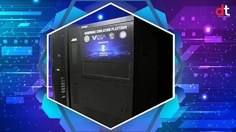
Comprising of Veloce Apps, Veloce Strato hardware & OS, and Veloce Protocol Solutions, Veloce from Siemens owns a “compute facility of 128 CPU cores and capacity of 640 million gates.” This is designed to address the challenges come across the designers of critical system on a chip (SoCs) and integrated circuit (highly sophisticated IC).
“We were receiving the huge demand from students, researchers, faculty members & entrepreneurs across the country in respect of further enhancing & extending the EDA & design solutions from Siemens to more organizations. The enhanced support from Siemens at the ChipIN Centre will play a crucial role in fulfilling the vision of turning India into a semiconductor powerhouse,” said Ms. Sunita Verma, Group Coordinator (R&D in Electronics & IT), Ministry of Electronics and IT.
“India today presents a significant opportunity for aspiring entrepreneurs and researchers to be at the forefront of designing and redefining the semiconductor systems, devices and products of the future. Siemens is proud to extend its participation in the “Chips to Start-up (C2S) Programme” of Government of India and MeitY by expanding access of its state-of-the-art EDA technology solutions to 250 educational institutions across India.
Our contribution is a testament of alignment with the nation's unwavering commitment to building a robust and self-sustaining semiconductor ecosystem by empowering the next generation of engineers, researchers and entrepreneurs to drive India's technological advancements and propel the nation towards becoming a global powerhouse,” said Ruchir Dixit, Vice President & Country Manager, EDA, Siemens Digital Industries Software.
𝐒𝐭𝐚𝐲 𝐢𝐧𝐟𝐨𝐫𝐦𝐞𝐝 𝐰𝐢𝐭𝐡 𝐨𝐮𝐫 𝐥𝐚𝐭𝐞𝐬𝐭 𝐮𝐩𝐝𝐚𝐭𝐞𝐬 𝐛𝐲 𝐣𝐨𝐢𝐧𝐢𝐧𝐠 𝐭𝐡𝐞 WhatsApp Channel now! 👈📲
𝑭𝒐𝒍𝒍𝒐𝒘 𝑶𝒖𝒓 𝑺𝒐𝒄𝒊𝒂𝒍 𝑴𝒆𝒅𝒊𝒂 𝑷𝒂𝒈𝒆𝐬 👉 Facebook, LinkedIn, Twitter, Instagram
