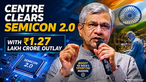

The Centre has formally notified Semicon 2.0, putting into operation its ambitious ₹1.27 lakh crore semiconductor programme aimed at expanding India’s capabilities across the entire semiconductor value chain. The new framework moves the country’s semiconductor strategy beyond fabs and assembly towards chip design, intellectual property, equipment, materials, advanced packaging, research and development, and talent development.
The notification by the Ministry of Electronics and Information Technology (MeitY) comes after the Union Cabinet approved Semicon 2.0 in July. The programme has been structured around six pillars and 10 categories, significantly widening the scope of companies and institutions that can participate. Startups, MSMEs, semiconductor manufacturers, packaging companies, equipment and materials makers, research organisations and training institutions are among those expected to benefit.
The move comes at a critical point for the global semiconductor industry. The rapid expansion of AI, data centres, advanced computing, automotive electronics and connected devices is driving demand for increasingly sophisticated chips. At the same time, geopolitical tensions and supply-chain vulnerabilities have pushed countries to reduce dependence on concentrated manufacturing hubs and build resilient domestic semiconductor capabilities.
IT Secretary S. Krishnan said the time was right for India to move to the next stage of semiconductor development, with self-reliance and the creation of a globally competitive industry forming the core objectives of Semicon 2.0.
Six Pillars to Build a Complete Chip Ecosystem

Semicon 2.0 covers six broad areas: chip design; semiconductor equipment and materials; semiconductor fabrication; assembly, testing, marking and packaging (ATMP); research and development; and talent development.
The wider approach is significant because a competitive semiconductor industry cannot depend only on fabrication plants. It requires a supporting network of equipment manufacturers, materials suppliers, packaging companies, chip-design firms, IP developers, research institutions and skilled professionals.
The design pillar is expected to provide greater support to startups and companies developing commercial semiconductor products. Eligible startups can receive financial assistance through grants and equity co-investment, while companies can access royalty financing or equity co-investment.
Up to 40% Support for Silicon Fabs
One of the biggest provisions under Semicon 2.0 is financial assistance for new semiconductor fabrication facilities. The government will provide up to 40% of eligible capital expenditure for silicon wafer fabs. Compound semiconductor, display and other specialised fabs, including LCD, OLED and Micro LED facilities, can receive support of up to 35% of eligible capex.
The revised support structure is aimed at encouraging large-scale private investment while maintaining significant government participation in capital-intensive semiconductor manufacturing projects.
Major Push for Advanced Packaging
Semicon 2.0 also gives substantial attention to semiconductor packaging, an increasingly important part of modern chip manufacturing. Advanced packaging projects will be eligible for support of up to 35% of eligible capital expenditure, while conventional packaging projects can receive support of up to 25%.
The focus on advanced packaging is particularly relevant to AI and high-performance computing. As chip architectures become more complex, technologies such as 2.5D and 3D packaging and heterogeneous integration are becoming increasingly important for improving computing performance and efficiency.
Strengthening India’s Chip Design Capabilities
The government is also looking to strengthen India’s position in semiconductor design. Under the first phase of the programme, several design projects and startups were supported, creating a foundation for a larger domestic chip-design ecosystem.
Semicon 2.0 seeks to build on that foundation by encouraging the development of semiconductor intellectual property, system-on-chips and modules for commercial as well as strategically important applications.
Research and Talent Take Centre Stage
Research and talent development form another important component of the new programme. Semiconductor manufacturing requires highly specialised expertise, from chip architecture and fabrication to packaging, materials and equipment.
According to the government, India has already developed around 85,000 semiconductor engineers, exceeding its earlier target ahead of schedule. The next phase aims to further expand the talent pool, including a target of developing 100,000 semiconductor design engineers over the coming years. This focus is designed to address one of the industry's biggest long-term challenges: ensuring that India has the specialised workforce required to support a growing semiconductor ecosystem.
Building on Semicon 1.0
Semicon 2.0 builds on the projects approved under the first phase of India's semiconductor programme. The government had approved 12 semiconductor projects across six states, representing cumulative investments of more than ₹1.64 lakh crore. These projects include a silicon fabrication facility, a silicon carbide fab, a gallium nitride-based Micro LED display fab and multiple semiconductor packaging facilities.
Three projects involving Micron, Kaynes Semicon and CG Semi have already commenced commercial production, providing an important foundation for the next phase of the country's semiconductor strategy.
India Targets a Larger Role in Global Semiconductor Supply Chains
The government expects Semicon 2.0 to catalyse substantial private-sector investment and strengthen India's position in the global semiconductor value chain. The programme has been designed as a multi-year initiative, with applications initially open for three years and supported projects extending over a longer implementation period.
The India Semiconductor Mission will serve as the nodal agency for the programme, overseeing applications, evaluation, recommendations and implementation.
The larger ambition is to move India beyond being a major consumer of semiconductor-powered products and establish the country as a meaningful global hub for chip design, manufacturing, packaging, research and semiconductor supply.
With Semicon 2.0, the government is now shifting its focus from building individual semiconductor facilities to creating an interconnected ecosystem around them. The success of the programme will ultimately depend on execution—attracting global semiconductor players, scaling Indian chip-design companies, developing domestic equipment and materials capabilities, creating specialised talent and integrating Indian manufacturing deeper into global supply chains.
𝐒𝐭𝐚𝐲 𝐢𝐧𝐟𝐨𝐫𝐦𝐞𝐝 𝐰𝐢𝐭𝐡 𝐨𝐮𝐫 𝐥𝐚𝐭𝐞𝐬𝐭 𝐮𝐩𝐝𝐚𝐭𝐞𝐬 𝐛𝐲 𝐣𝐨𝐢𝐧𝐢𝐧𝐠 𝐭𝐡𝐞 WhatsApp Channel now! 👈📲
𝑭𝒐𝒍𝒍𝒐𝒘 𝑶𝒖𝒓 𝑺𝒐𝒄𝒊𝒂𝒍 𝑴𝒆𝒅𝒊𝒂 𝑷𝒂𝒈𝒆𝐬 👉 Facebook, LinkedIn, Twitter, Instagram
