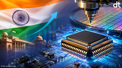

The Union Cabinet has approved Semicon 2.0 with a budgetary outlay of ₹1,27,500 crore, marking the government's next major step towards building a globally competitive semiconductor ecosystem in India. The initiative builds on the progress achieved under the India Semiconductor Mission (ISM) and aims to strengthen the country's capabilities across semiconductor design, manufacturing, research, advanced packaging, materials, equipment, and talent development.
The new programme reflects the government's long-term commitment to positioning India as a strategic destination for semiconductor innovation and manufacturing while reducing dependence on global supply chains for critical technologies.
Six Pillars to Build a Complete Semiconductor Ecosystem
Semicon 2.0 has been designed around six strategic pillars that cover the entire semiconductor value chain.
The first pillar focuses on semiconductor design. Building on the momentum created by more than 100 startups already working on chip development, the programme will support the creation of intellectual property (IP), advanced chip designs and system-level innovations for both commercial and strategic applications. The government aims to establish India as a globally recognised semiconductor IP and chip design hub.
The second pillar aims to strengthen the domestic ecosystem for semiconductor manufacturing equipment, specialty chemicals, gases and advanced materials. Companies engaged in manufacturing these critical inputs as well as related R&D activities will receive incentives to develop a sustainable semiconductor supply chain within the country.
More Chip Fabs and Advanced Packaging Facilities
A key focus of Semicon 2.0 is expanding semiconductor manufacturing capacity in India. Following the approval of the country's first semiconductor fabrication plants, the government plans to attract additional investments in silicon fabs, compound semiconductor fabs, discrete component manufacturing units, display fabs and other advanced chip manufacturing facilities.
The programme will also continue supporting the growth of Assembly, Testing, Marking and Packaging (ATMP) and Outsourced Semiconductor Assembly and Test (OSAT) facilities. With global semiconductor companies increasingly exploring India as an alternative manufacturing destination, the government aims to bring advanced packaging technologies into the country while strengthening domestic production capabilities.
R&D and Talent Development Receive Major Push
Research and development forms another key pillar of Semicon 2.0. While India's semiconductor journey initially focuses on mature process nodes ranging from 28nm to 110nm, the new programme seeks to support research into more advanced semiconductor technologies through collaborations with leading research institutions in India and abroad.
Talent development also remains central to the initiative. The government plans to deepen semiconductor education across universities while expanding industry participation in specialised training related to chip fabrication, cleanroom operations, semiconductor manufacturing and ecosystem development.
Currently, over 315 universities are training students using industry-standard Electronic Design Automation (EDA) tools, with nearly 68,000 students already receiving semiconductor design training.
Building on the Success of Semicon 1.0
The approval of Semicon 2.0 comes after significant progress under the first phase of the India Semiconductor Mission.
According to official information, the government has approved 12 semiconductor manufacturing projects involving cumulative investments exceeding ₹1.64 lakh crore. These include one silicon fabrication plant, one silicon carbide fab, an integrated gallium nitride Micro LED display fab, and nine semiconductor packaging facilities catering to industries such as consumer electronics, automotive, telecommunications, industrial electronics, aerospace and power electronics.
Commercial production has already commenced at facilities operated by Micron, Kaynes and CG Semi, while another approved project is expected to begin production during 2026.
On the design front, 24 semiconductor design projects from startups and MSMEs have received financial support, while 105 startups have gained access to advanced EDA design tools. These companies are developing chips for applications including artificial intelligence, IoT devices, telecom equipment, satellite communications, drones, surveillance systems and smart metering.
Strengthening India's Position in the Global Semiconductor Industry
The government believes Semicon 2.0 will help strengthen India's technological capabilities, improve supply chain resilience, generate high-value employment and accelerate economic growth across multiple sectors. By supporting the complete semiconductor value chain—from design and research to manufacturing and packaging—the programme aims to position India as a significant player in the rapidly evolving global semiconductor industry while supporting the country's broader vision of technology self-reliance and innovation-led growth.
𝐒𝐭𝐚𝐲 𝐢𝐧𝐟𝐨𝐫𝐦𝐞𝐝 𝐰𝐢𝐭𝐡 𝐨𝐮𝐫 𝐥𝐚𝐭𝐞𝐬𝐭 𝐮𝐩𝐝𝐚𝐭𝐞𝐬 𝐛𝐲 𝐣𝐨𝐢𝐧𝐢𝐧𝐠 𝐭𝐡𝐞 WhatsApp Channel now! 👈📲
𝑭𝒐𝒍𝒍𝒐𝒘 𝑶𝒖𝒓 𝑺𝒐𝒄𝒊𝒂𝒍 𝑴𝒆𝒅𝒊𝒂 𝑷𝒂𝒈𝒆𝐬 👉 Facebook, LinkedIn, Twitter, Instagram
